Categories
- High Power LED
- COB LEDs
- LED Grow Light Chip
- LED Driver
- LED Flood Lights
- LED Power
- LED Switching Power Supply
- Top High Power LEDs
- LED Lights & Lighting
- LED Bulb
- LED Energy Saving Lamps
- LED Logo Projector Lights
- LED Street Lights
- LED Strip Lights
- Led Strip Lights 5V USB
- New Products ...
- Featured Products ...
- All Products ...
Technical Support
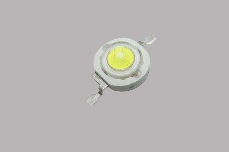
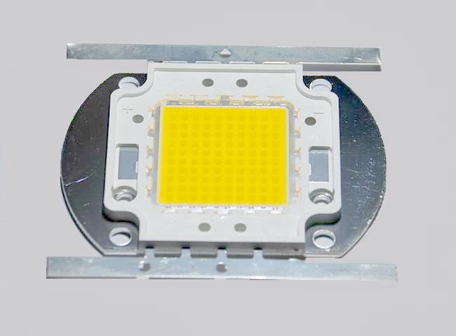
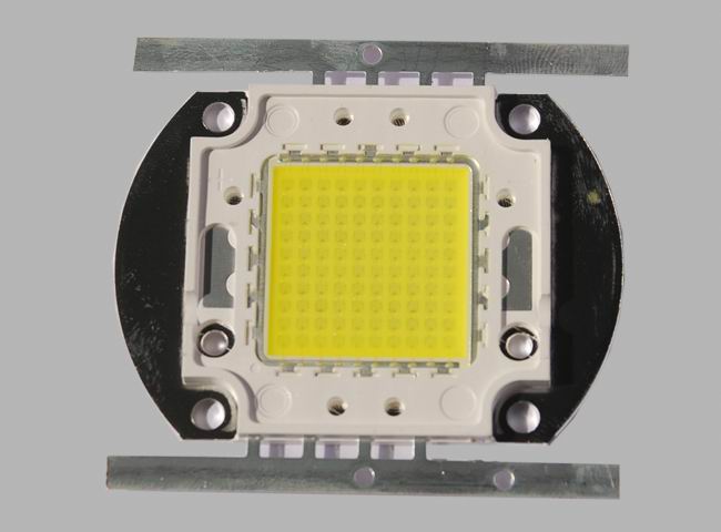
High-power LED packaging technology and development trends 1, Introduction: High-power LED package structure and process because of the complex, and a direct impact on the use of high-power LED performance and life, has been a research hotspot in recent years, especially in high-power white light LED package is research hotspot in hot spots. High-power LED package features include: 1. Mechanical protection to improve reliability; 2. To enhance heat dissipation in order to reduce the chip junction temperature, improve the performance of high-power LED; 3. Optical control, improve light efficiency and optimize the beam distribution ; 4. power supply management, including AC / DC change, as well as power control. High-power LED packaging methods, materials, structure and process of selection by the chip structure, photoelectric / mechanical properties, the specific application and cost factors. After 40 years of development, LED package has undergone Scaffolding (Lamp LED), patch type (SMD LED), high-power LED-based (Power LED), such as stage of development. With the chip power increases, especially in solid-state lighting technology development needs of high-power LED package, optical, thermal, electrical and mechanical structure of a new and higher requirements. In order to effectively reduce the package thermal resistance, improve the efficiency of the light, we must adopt a new technology for packaging design ideas. Second, the key to high-power LED packaging technology: high-power LED package mainly related to light, heat, electric, structure and process, etc., as shown in Figure 1. Both of these factors with each other independent of each other and affect each other. One of just the purpose of LED packaging, heat is the key, electric, structure and process is the means, while the level of performance is a concrete manifestation of package. Compatibility from the process and reduce production costs, the high-power LED packaging design should be carried out simultaneously with the chip design, chip design that should be taken into account when the package structure and process. Otherwise, such as chip manufacturing is completed, probably because of the need for a chip package structure, and thereby extend the product cycle and technology R & D costs, and sometimes even impossible. In particular, high-power LED package of key technologies include: (1) low thermal resistance packaging technology: With regard to the existing high-power LED luminous efficiency levels, because of the importation of about 80% of electrical energy into heat, and high-power LED chip size, therefore, are high-power LED chip cooling package must address the key issues. Mainly include the chip layout, packaging materials selection (substrate material, thermal interface materials) and technology, heat sink design. High-power LED thermal resistance package includes materials (substrate and heat sink thermal structure) internal resistance and the interfacial thermal resistance. The role of heat is absorbed substrate chip heat generated and transmitted to the heat sink on, implementation of the heat exchange with the outside world. Thermal Materials commonly used substrates including silicon, metals (such as aluminum, copper), ceramic (eg, AlN, SiC) and composite materials. Such as Nichia Corporation's third-generation LED make using CuW substrate will be 1mm at CuW flip chip substrates, reduces the package thermal resistance, improve the high-power LED light-emitting power and efficiency; Lamina Ceramics Company developed a low temperature cofired Ceramic metal substrate, as shown in Figure 2 (a), and the development of the corresponding high-power LED packaging technology. First of all, the technology prepared eutectic solder is suitable for high-power LED chips and the corresponding ceramic substrate, and then high-power LED chip and substrate directly welded together. Because of the substrate integrated eutectic solder layer, electrostatic protection circuit, drive circuit and control compensation circuit, not only simple in structure, but also because of high thermal conductivity materials, thermal interface less, greatly improving the thermal performance for high-power LED Array out package put forward solutions. Germany developed Curmilk high thermal conductivity copper ceramic plates, ceramic substrates by the (AlN) and conductive layer (Cu) at high temperature and high pressure sintering formed, there is no use of bonding agents, so good thermal conductivity, high strength, insulation, and Figure 2 (b) below. One of aluminum nitride (AlN) for the thermal conductivity 160W/mk, coefficient of thermal expansion (with the thermal expansion coefficient of silicon equivalent), which reduces the package thermal stress. Studies have shown that the interface of the package thermal resistance is also a great influence, if not correctly handle the interface, on access to good cooling effect. For example, room temperature, good interfacial contact at the interface under high temperature gap may exist, substrate warpage may also affect the bonding and local cooling. To improve the high-power LED package, the key is to reduce the interface and the interface thermal contact resistance and enhance heat dissipation. Therefore, the chips and hot thermal interface between the substrate material (TIM) selection is very important. High-power LED package commonly used in TIM and thermal conductivity for the conductive adhesive gel, because of low thermal conductivity, generally 0.5-2.5W/mK, resulting in high interfacial thermal resistance. The use of low temperature or eutectic solder, solder paste or nanoparticles doped with conductive adhesive as a hot interface materials, can greatly reduce the interfacial thermal resistance. (B) the high rate of take-ray package structure and process: At high-power LED use, generated by photon radiation compound fired at from outside, caused by the loss, mainly include three aspects: the internal structure of the chip defect as well as the material absorption; photon At the radio interface because of the refractive index of the reflection loss caused by bad; and because of the incident angle greater than the total reflection critical angle of total reflection caused by the loss. Therefore, a lot of light can not reach from outside the chip. Through the surface coating layer of the chip at a relatively high refractive index transparent layer (Potting), because of the layer in between the chip and air, thus effectively reduce the photon loss at the interface, improve the efficiency of the check light. In addition, the role of Potting chip also includes a mechanical protection, stress release, and as a light guide structure. Therefore, the requirements of its high transmittance, high refractive index, thermal stability, good fluidity, easy to spray. To improve the reliability of high-power LED package, also called potting materials with low moisture absorption, low-stress, anti-aging properties. Potting currently used, including epoxy resin and silica gel. Because silicone has a high transmittance, refractive index, and thermal stability, stress, low moisture absorption characteristics, is superior to epoxy resin, at high-power LED package is widely used, but higher costs. Studies have shown that improve the refractive index of silica gel can effectively reduce the refractive index of the physical barrier caused by photon losses, improve external quantum efficiency, but the performance of silica gel influenced by environmental temperature. As the temperature increases, the silica gel inside the thermal stress to increase, resulting in lowering the refractive index of silica gel, thus affecting the high-power LED light efficiency and light intensity distribution. The role of phosphor is light colored composite, the formation of white light. Its characteristics include particle size, shape, light-emitting efficiency, conversion efficiency, stability (thermal and chemical), etc., in which light-emitting efficiency and conversion efficiency is the key. Research shows that with an increase in temperature, phosphor quantum efficiency, light reduction, radiation wavelength Change will happen, thus giving rise to high-power white LED color temperature, color changes, a higher temperature will accelerate the aging of phosphors. Due to the phosphor coating by epoxy or silicone and phosphor from the deployment, lower heat dissipation, when the subject here or UV radiation, the prone to quenching temperature and aging, so that light-emitting efficiency . In addition, under high temperature and phosphor Potting thermal stability is also problematic. Phosphors commonly used because of the size at more than 1um, refractive index greater than or equal to 1.85, while the silica refractive index is normally around 1.5. Between them because of refractive index mismatch, as well as the phosphor particle size is much larger than light-scattering limit (30nm), and therefore exist in the phosphor particle surface light scattering, reduces the light efficiency. Through the incorporation of nano-silica gel phosphor can improve the refractive index of 1.8 or above to reduce light scattering, improve the efficiency of high-power LED light (10% -20%), and can effectively improve the quality of light color. Phosphor coating the traditional way is to phosphor with Potting mix, then coated on the chip. Unable to because of the phosphor coating thickness and shape for precise control of color led to Exit inconsistent, partial emergence of Blu-ray or optical. And Lumileds developed Conformal coating (Conformal coating) technology can achieve uniform phosphor coating to protect the light color uniformity, in Figure 3 (b). But research shows that when the direct phosphor coating on the chip surface, because of the existence of light scattering, light and less efficient. In view of this, the United States Institute Rensselaer a photon scattering extraction process (Scattered Photon Extraction method, SPE), at the chip surface through a focusing lens arrangement, and containing phosphor under glass away from the location of the chip must not only improve the device reliability, but also greatly improve the luminous efficiency (60%), Figure 3 (c). Generally speaking, in order to improve high-power LED light of the efficiency and reliability, packaging layer has been gradually transparent high refractive index glass or glass-ceramics, such as replacing the trend through the phosphor within the doped or treated glass surface, not only improve the evenness of the phosphor, but also improve the efficiency of the package. In addition, the reduction of high-power LED light direction of the number of optical interfaces, but also improve the efficiency of the optical effective measures. (C) the array package and system integration technology: after 40 years of development, LED packaging technology and structure has undergone four stages, shown in Figure 4. 1, pin-type (Lamp) LED Packaging: pin package is commonly used in the structure of 3-5mm package. Generally used for smaller current (20-30mA), low power (less than 0.1W) of the LED package. Mainly used for instrument display or instructions, a large-scale integration can also be used as display. Its disadvantage is that the larger package thermal resistance (generally higher than 100K / W), short-lived. 2, Surface Mount (SMD) Type (SMT-LED) Packaging: Surface Mount Technology (SMT) is a good device directly to the package paste, solder to the PCB the specified location on the surface of a packaging technology. In particular, is to use a particular instrument or equipment will be pre-coated chip pin at the adhesive and solder paste graphics on the pad, then mount directly to the non-drilled mounting holes on the surface of the PCB after wave soldering or after reflow soldering, so that devices and circuits set up between the reliable mechanical and electrical connections. SMT technology and high reliability, high-frequency characteristics of a good, easy to realize the advantages of automation, the electronics industry are one of the most popular packaging technologies and processes. 3, straight-chip-mounted board (COB) LED Packaging: COB are Chip On Board (on-board chip fitted straight) English acronym is a kind of glue or solder through the LED chip to paste it directly into the PCB board, through wire bonding chip and PCB implementation cubicle electric interconnection packaging technology. PCB board can be a low-cost FR-4 material (glass fiber reinforced epoxy resin), it could be a high thermal conductivity of metal matrix or ceramic matrix composites (such as aluminum or copper plate ceramic substrate, etc.). And wire bonding using high temperature thermal bonding (gold wire welding) and under normal temperature and ultrasonic bonding (welding aluminum chopper). COB technology mainly used for high-power multi-chip LED array package with SMT, compared not only greatly improve the power density packaging, and reduces the thermal resistance package (normally 6-12W/mK). 4, the system Encapsulated (SiP) LED Packaging: SiP (System in Package) in recent years to adapt to a portable machine and system development requirements of miniaturization, in system-on-chip System on Chip (SOC) developed on the basis of a new way of packaging integration. SiP-LED on the run, not only in a package assembled a number of light-emitting chips, can also be a variety of different types of devices (such as power supply, control circuitry, optical micro-structures, sensors, etc.) integrated together, to build into a more complex and complete systems. Structure compared with other packages, SiP has good process compatibility (can use existing electronic packaging materials and processes), high integration, low cost, can provide more new features, easy to sub-block test, short development cycle and so on. In accordance with the different type of technology, SiP can be divided into four: chips stacked type, module type, MCM-type and three-dimensional (3D) package type. At present, high-power high-brightness LED devices to replace the incandescent and high pressure mercury lamp, we must enhance the total luminous flux, or luminous flux can be used. The increase in flux can improve integration, increase the current density, the use of large-size chips and other measures to achieve. Which will increase the power density of high-power LED, such as thermal poor will lead to high-power LED chip junction temperature rise, thus directly affecting the performance of LED devices (such as light-emitting efficiency, Exit happen redshift, lower life expectancy, etc. ). Multi-chip array package is the high flux of one of the most viable option, but the density of LED array package is subject to price, available space, electrical connections, especially the heat and so on. Because of light-emitting chip, high-density integration, cooling substrate temperature on high, must adopt effective heat sink structure and the appropriate packaging technology. Commonly used heat sink structure is divided into passive and active cooling. General selection of passive cooling with a high coefficient of the fin rib, through the fin and air natural convection between the heat dissipation into the environment. The program structure is simple, high reliability, but because of natural convection heat transfer coefficient of a lower power density can only be applied to lower integration is not high. For high-power LED package, it must be active cooling, such as Fin + fan, heat pipe, liquid forced convection, micro-channel cooling, phase change, such as refrigeration. At system integration, Taiwan Xinqiang optoelectronic systems packaging technology company (SiP), and through fin + heat pipe with a highly efficient way of cooling modules, developed the 72W, 80W high-power high-brightness white LED light source, Figure 5 (a). Because of the lower package thermal resistance (4.38 ℃ / W), when the ambient temperature of 25 ℃, high-power LED junction temperature control at below 60 ℃, thus ensuring a high-power LED service life and good luminescent properties. And Huazhong University of Science and Technology is used initiative COB packaging and cooling technology, packaging a 220W and 1500W ultra-high-power white LED light source, Figure 5 (b). (Iv) package large-scale production technology: Wafer bonding (Wafer bonding) technology refers to the structure and the circuit chip production, are in the chip package (Wafer) up, and package after the completion of cutting, forming a single chip ( Chip); corresponding to the die bonding, refers to the structure and chips at the chip on the circuit is completed, that is the formation of cutting chips (Die), then on a single chip package (similar to the existing high-power LED packaging technology ), as shown in Figure 6. Obviously, the wafer bonding package efficiency and higher quality. Because of packaging costs at high-power LED device manufacturing costs accounted for a large proportion, therefore, to change the existing high-power LED package (from the die bonding to the wafer bonding), will greatly reduce the manufacturing cost package. In addition, wafer bonding package can also improve the production of high-power LED devices cleanliness to prevent bonding before dicing, slicing process on the device structure of the damage, improve yield and reliability of packaging, which is a lower cost-effective means of packaging. In addition, high-power LED package, must be at chip design and packaging design process, as far as possible, using less technology package (Package-less Packaging), at the same time simplify the package structure, as far as possible to reduce the thermal and optical interface number in order to reduce the package thermal resistance, improve the efficiency of the light. (Friday) package reliability testing and assessment: high power LED device failure modes include electricity failure (such as short circuit or open circuit), light failure (such as high temperature caused by Potting yellow, optical performance degradation, etc.) and mechanical failure (such as lead fracture, etc.), and these factors have with the package structure and process-related. High-power LED's life time average failure (MTTF) to define, for lighting purposes, generally refers to high-power LED output flux attenuation for the initial 70% (for display purposes generally defined as the initial value of 50%) the use of time. Because of high-power LED long life, usually taken to accelerate the environmental test the reliability of the method of testing and evaluation. The contents of the tests include high temperature storage (100 ℃, 1000h), low temperature storage (-55 ℃, 1000h), high temperature and humidity (85 ℃ / 85%, 1000h), cycle of high and low temperature (85 ℃ ~ -55 ℃), thermal shock corrosion resistance, anti-soluble, such as mechanical impact. However, accelerated environmental testing is only one aspect of the issue of high-power LED lifetime prediction mechanism and methods of research are still problems to be examined. Third, solid-state lighting to high-power LED package requirements: Compared with traditional lighting, high power LED lamps do not require the use of filters or filter to produce light have not only high efficiency, light color purity, and can achieve Dynamic or gradual color changes. Change the color temperature at the same time maintain a high color-rendering index, necessary to meet the different applications. However, its package also put new demands, embodied in: (1) Modularity: the adoption of a number of high-power LED lamp (or module) can achieve the interconnected lumens output superposition good to meet the requirements of high-brightness lighting . Through modular technology, can be a number of points or high-power LED light source module in accordance with the random combination of shapes to meet the lighting requirements of different areas. (B) to maximize system efficiency: In order to improve high-power LED lamps light efficiency, apart from a suitable high-power required LED power supply, it is also necessary to adopt efficient cooling structure and process, as well as the optimization of internal / external optical design in order to improve the entire system efficiency. (C) low-cost: high-power LED lamps to move towards the market, must be on at the cost of competitive advantage (mainly refers to the initial installation costs), while the package in the entire high-power LED lighting production costs accounted for a very large, therefore, the use of new package structure and technology, enhance luminous efficiency / cost ratio and achieve high-power LED lamps are the key to commercialization. (Iv) easy replacement and maintenance: high-power LED light source because of long life and low maintenance costs, and therefore high-power LED lighting package higher reliability requirements. Require high-power LED lighting design is easy to adapt to the future to improve the efficient high-power LED chip packaging requirements and the requirements of interchangeability LED chip is better in order to facilitate the lighting manufacturers adopted its own chip select. High-power LED light source lamp can be composed of multiple distributed point light source, because of chip size small, so that the package of the lamp light weight, compact structure, and to meet a variety of shapes and different integration requirements. The only shortage is that there is no ready-made design standards, but at the same time give the design provides ample room for imagination. In addition, the high-power LED lighting control are the primary objective of supply. Because in general the city are high-voltage alternating current electric power (220V, AC), which required high-power LED constant current or current-limiting power supply, which necessitates the use of the conversion circuit or embedded control circuitry to achieve an advanced calibration and closed-loop feedback control system. In addition, digital lighting control technology, the use of solid-state light sources and control of major depend on intelligent control and management software to achieve, thus the user, information and light source set up a new inter-linked, and can give full play to the imagination of designers and consumers force. IV Conclusion: High-power LED package is a related to many disciplines (such as optical, thermal, mechanical, electrical, mechanical, materials, semiconductors, etc.) study. In some ways, the high-power LED package is not only a manufacturing technology (Technology), but also a basic science (Science), a good package for the necessary hot study, optical, materials and processes, such as the physical nature of mechanical understanding and application. High-power LED packaging design should be carried out simultaneously with the chip design and the need to light, heat, electricity, structural considerations, such as a unified performance. At packaging process, although the material (heat dissipation substrate, phosphor, Potting) selection is very important, but the package structure (such as hot learn interface, optical interface) for high-power LED luminous efficiency and reliability of a great impact white high-power LED package must adopt new materials and new technologies and new ideas. For high-power LED lamps, the more are required to source, heat, electricity and lighting, such as integrated consideration. |
Important Links
Who's Online
There currently are 19 guests online.
Copyright © 2008-2023 TAOYUAN ELECTRON (HK) LIMITED. Powered by Taoyuan LED
Website: www.8mpacc.com/en Skype: HK.company
E-Mail: ledwvv@gmail.com
Website: www.8mpacc.com/en Skype: HK.company
E-Mail: ledwvv@gmail.com


